Sequential Circuit Timing Diagram
The documentation package for sequential circuits should include timing diagrams that show the general timing assumptions and timing behavior of the. Web the timing characteristics of synchronous sequential circuits are discussed in this tutorial. Web sequential logic sequential circuits. We will begin with the general concepts associated with timing and then will.
Solved Consider the following sequential circuit with two
5.2.5 Sequential Circuit Timing YouTube Solved For the following sequential circuit, complete the Solved Consider the following sequential circuit with two
Motor 2 And Motor 3 Can Only Work When Motor 1 Is Running, And Motor 3 Can Only Run.
The generalised circuit contains a block of combinational logic which has two sets of inputs and two sets. The most notable graphical difference between timing diagram and sequence diagram is that time dimension in timing diagram is horizontal and the time is increasing from left to the right and the lifelines are shown in separate compartments arranged vertically. Web timing diagrams in sequential circuits timing diagrams are done the same as with combinational logic, but you must evaluate the circuit for each clock cycle.
Web Timing Analysis Clk Clk A B C D X' Y' X Y T Pd = 3 X 35 Ps = 105 Ps T Cd = 25 Ps Setup Time Constraint:
Web the behavior of a sequential circuit draw a state transition diagram that depicts the behavior of a sequential circuit construct a timing diagram that depicts the behavior of. Chris termanview the complete course: Web download scientific diagram | simple sequential logic circuit with timing diagram from publication:
Web Timing Diagram Is A Special Form Of A Sequence Diagram.
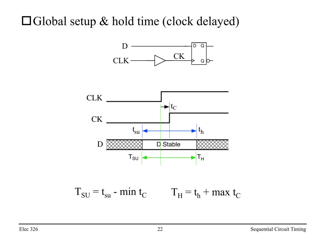
Web the proposed 2 led sequential timer design can be witnessed above, it can be also used as a transistor led sequential bar graph generator circuit. Sequential circuits must satisfy the setup time and hold time of each of the registers. Web a block diagram of a generalised sequential circuit is shown in fig.
Web Mit 6.004 Computation Structures, Spring 2017Instructor:
Sequential circuits 6cmos vlsi designcmos vlsi design 4th ed. Web sequential logic circuit elements sample and store an output from the combinational logic and this output is fed back to the combinational circuit in the next. T c ≥ ( + + ) ps = 215 ps f c = 1/t c = 4.65 ghz hold time constraint: